

TANMS memory testbed
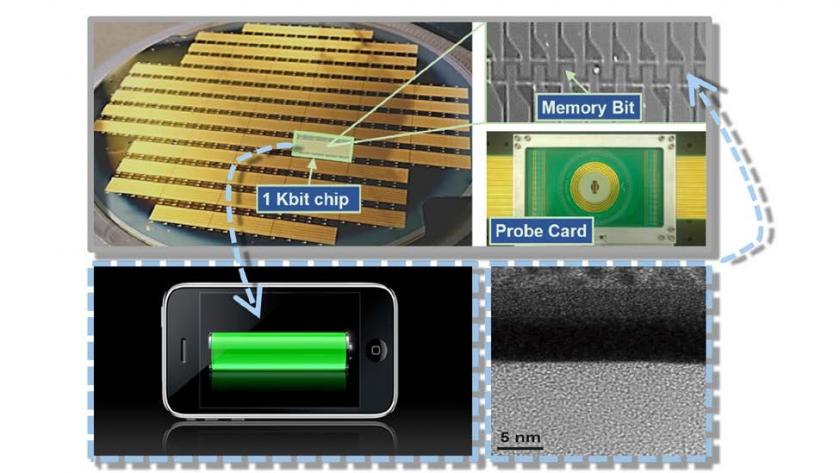
The TANMS memory testbed, from fundamentals to applications: Top panel:silicon wafer with memory chips plus close-up of individual bits; bottom right:cross-sectional image of multilayer structure used in memory elements; bottom left: smart phones with radically longer battery life exemplify some of the low-power systems this technology could enable.
Credit:
TANMS