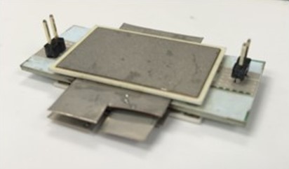
Novel 3D Power Module Package Building on Advantages of Silicon Carbide
Outcome/Accomplishment
A novel, 3D power module package for silicon carbide (SiC) power device was designed and fabricated by researchers at the Center for Power Optimization of Electro-Thermal Systems (POETS), an NSF-funded Engineering Research Center (ERC) based at the University of Illinois.
Impact/Benefits
This new packaging architecture helps build on the advantages of silicon carbide, including high switching speed, low switching loss, and ability to withstand high temperatures to enable high-frequency, high-temperature power electronics. The architecture reflects trends in SiC including optimized layout, advanced interconnection technologies, and efficient cooling system.
Explanation/Background
SiC metal-oxide-silicon field-effect transistors (MOSFETs) benefit from higher blocking voltage, lower on-state resistance, and higher thermal conductivity than their silicon counterparts. The enhanced performance is derived from the material advantages inherent in silicon-carbide physics of high-power and high-voltage semiconductor devices POETS's advanced module architecture goes beyond even most conceived 3D double-sided cooled modules by integrating cooling within an LTCC (low temperature co-fired ceramics) layer, providing 4-sided cooling. This approach leads to an effective heat transfer capability 3X-4X that of conventional 2D SiC commercial power modules. Further, the module boasts sub-nanoHenry parasitic inductances that are key to lower losses by an order of magnitude in high-frequency applications. This leads to higher efficiency, higher power density power converters that are 10X more power dense (> 100 kW/l) than previously commercialized.
The new architecture advanced earlier research by using non-conventional materials, including low-temperature, co-fired ceramics and nickel-plated copper balls. The optimized half-bridge module, based on common SiC MOSFET, used 3D power routing to minimize stray parasitic inductance. The module also used vertical and horizontal cooling paths to maximize heat dissipation.
Location
Urbana-Champaign, Illinoiswebsite
Start Year
Microelectronics and IT
Microelectronics, Sensing, and IT
Lead Institution
Core Partners
Fact Sheet
Outcome/Accomplishment
A novel, 3D power module package for silicon carbide (SiC) power device was designed and fabricated by researchers at the Center for Power Optimization of Electro-Thermal Systems (POETS), an NSF-funded Engineering Research Center (ERC) based at the University of Illinois.
Location
Urbana-Champaign, Illinoiswebsite
Start Year
Microelectronics and IT
Microelectronics, Sensing, and IT
Lead Institution
Core Partners
Fact Sheet
Impact/benefits
This new packaging architecture helps build on the advantages of silicon carbide, including high switching speed, low switching loss, and ability to withstand high temperatures to enable high-frequency, high-temperature power electronics. The architecture reflects trends in SiC including optimized layout, advanced interconnection technologies, and efficient cooling system.
Explanation/Background
SiC metal-oxide-silicon field-effect transistors (MOSFETs) benefit from higher blocking voltage, lower on-state resistance, and higher thermal conductivity than their silicon counterparts. The enhanced performance is derived from the material advantages inherent in silicon-carbide physics of high-power and high-voltage semiconductor devices POETS's advanced module architecture goes beyond even most conceived 3D double-sided cooled modules by integrating cooling within an LTCC (low temperature co-fired ceramics) layer, providing 4-sided cooling. This approach leads to an effective heat transfer capability 3X-4X that of conventional 2D SiC commercial power modules. Further, the module boasts sub-nanoHenry parasitic inductances that are key to lower losses by an order of magnitude in high-frequency applications. This leads to higher efficiency, higher power density power converters that are 10X more power dense (> 100 kW/l) than previously commercialized.
The new architecture advanced earlier research by using non-conventional materials, including low-temperature, co-fired ceramics and nickel-plated copper balls. The optimized half-bridge module, based on common SiC MOSFET, used 3D power routing to minimize stray parasitic inductance. The module also used vertical and horizontal cooling paths to maximize heat dissipation.

