A Revolutionary Type of Data Storage Device
Outcome/Accomplishment
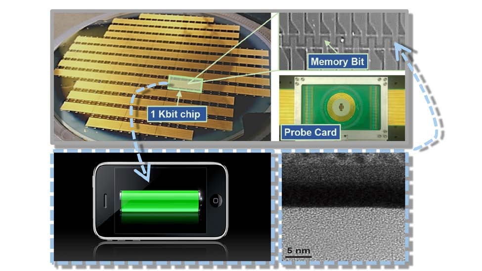
Researchers at the NSF-funded Nanosystems Engineering Research Center (ERC) for Translational Applications of Nanoscale Multiferroic Systems (TANMS), led by the University of California Los Angeles (UCLA), have developed a revolutionary new type of magneto-electric memory (data storage) device—a breakthrough in the semiconductor industry. The memory (see figure) has been demonstrated on 1 kilobit (Kbit) array prototypes built and tested by the TANMS team.
Impact/Benefits
This new memory is a strong candidate to replace several existing types of memory, particularly SRAM and DRAM, thereby continuing their sustained progress and cost reduction while delivering significantly improved performance, such as a 1,000-fold write energy reduction (a revolutionary advancement because power consumption is a major constraint in existing memories). The new memory also enables new architectures for computing, from green computers to information processors that consume very little or no standby power (i.e., instant-on-demand).
Explanation/Background
There are, in addition, far-reaching implications well beyond longer-life portable devices and extending to various embedded and stand-alone memory and logic chips, enabling lower-power data storage with fast access and high reliability. This achievement puts TANMS, and U.S. academic research generally, at the forefront of worldwide efforts in the emerging area of electric-field control of magnetic memory technology.
These efforts are expected to have a large, long-term impact on the >$60B memory market and perhaps on other parts of the $300B semiconductor industry. Several key industry members, both established and emerging companies, have expressed interest and are beginning to work with TANMS on transferring the technology to the marketplace.
The multi-disciplined, collaborative TANMS team previously demonstrated single-bit operation of the new memory device, and has now successfully demonstrated operation at a level of several Kbits, a key requirement to show feasibility for potential products. The TANMS technologies are based on a new class of emerging materials, termed multiferroics, in which electric fields (i.e., voltages) are used to change magnetic properties—for example, to realize ultra-small, nanoscale, magnetic switches, which can then be used to store information; using voltage is key to enabling reduced power dissipation and other benefits.
To create the memory device, researchers designed, fabricated, and tested voltage-controlled magneto-electric tunnel junctions, where writing of information (i.e., switching of the magnetic storage element) is performed by fast pulses of voltage applied to the device. The applied voltage exerts a torque on the magnetization, the magnetic state is changed, bits in the memory array provide a readout mechanism, and the overall result is a functional memory testbed with non-volatile storage of information and ultra-low-power.
Location
Los Angeles, Californiawebsite
Start Year
Microelectronics and IT
Microelectronics, Sensing, and IT
Lead Institution
Core Partners
Fact Sheet
Outcome/Accomplishment
Researchers at the NSF-funded Nanosystems Engineering Research Center (ERC) for Translational Applications of Nanoscale Multiferroic Systems (TANMS), led by the University of California Los Angeles (UCLA), have developed a revolutionary new type of magneto-electric memory (data storage) device—a breakthrough in the semiconductor industry. The memory (see figure) has been demonstrated on 1 kilobit (Kbit) array prototypes built and tested by the TANMS team.
Location
Los Angeles, Californiawebsite
Start Year
Microelectronics and IT
Microelectronics, Sensing, and IT
Lead Institution
Core Partners
Fact Sheet
Impact/benefits
This new memory is a strong candidate to replace several existing types of memory, particularly SRAM and DRAM, thereby continuing their sustained progress and cost reduction while delivering significantly improved performance, such as a 1,000-fold write energy reduction (a revolutionary advancement because power consumption is a major constraint in existing memories). The new memory also enables new architectures for computing, from green computers to information processors that consume very little or no standby power (i.e., instant-on-demand).
Explanation/Background
There are, in addition, far-reaching implications well beyond longer-life portable devices and extending to various embedded and stand-alone memory and logic chips, enabling lower-power data storage with fast access and high reliability. This achievement puts TANMS, and U.S. academic research generally, at the forefront of worldwide efforts in the emerging area of electric-field control of magnetic memory technology.
These efforts are expected to have a large, long-term impact on the >$60B memory market and perhaps on other parts of the $300B semiconductor industry. Several key industry members, both established and emerging companies, have expressed interest and are beginning to work with TANMS on transferring the technology to the marketplace.
The multi-disciplined, collaborative TANMS team previously demonstrated single-bit operation of the new memory device, and has now successfully demonstrated operation at a level of several Kbits, a key requirement to show feasibility for potential products. The TANMS technologies are based on a new class of emerging materials, termed multiferroics, in which electric fields (i.e., voltages) are used to change magnetic properties—for example, to realize ultra-small, nanoscale, magnetic switches, which can then be used to store information; using voltage is key to enabling reduced power dissipation and other benefits.
To create the memory device, researchers designed, fabricated, and tested voltage-controlled magneto-electric tunnel junctions, where writing of information (i.e., switching of the magnetic storage element) is performed by fast pulses of voltage applied to the device. The applied voltage exerts a torque on the magnetization, the magnetic state is changed, bits in the memory array provide a readout mechanism, and the overall result is a functional memory testbed with non-volatile storage of information and ultra-low-power.

